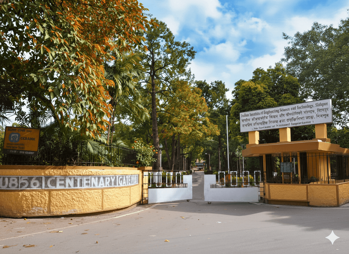
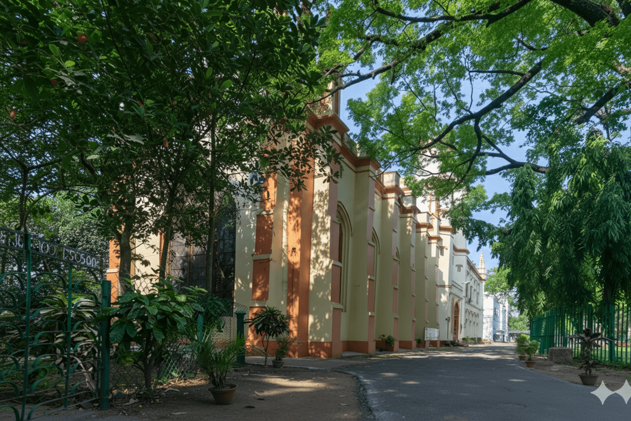
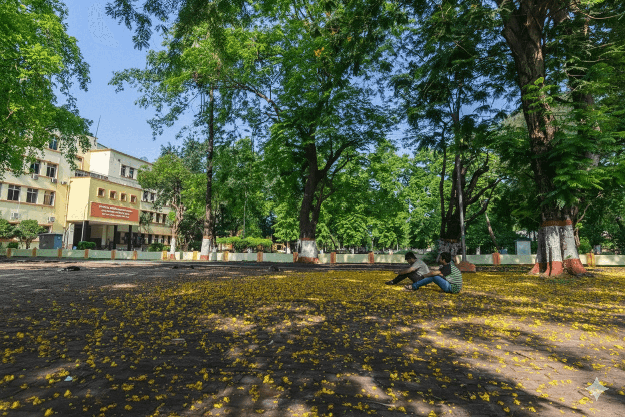
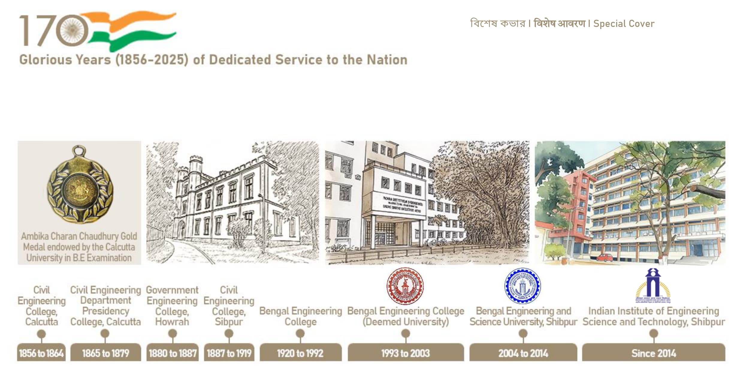
Pre-loader

Ananda Sankar Chakraborty

About


Dr. Ananda Sankar Chakraborty hails from Kolkata, India. He graduated from the West Bengal University of Technology, in Electronics and Communication Engineering (2004 - 2008). After several years of independent research work and consultancy along with a year working in the Software Industry, he joined the M.Tech program in VLSI design in Indian Institute of Engineering Science and Technology, Shibpur, India (2012 -14). During M.Tech, besides coursework he collaborated on various semiconductor based research problems and worked on a project sponsored by the Department of Atomic Energy, govt. of India. From 2014 - 2019 , he worked as a PhD researcher with the Department of Electronic Systems Engineering, Indian Institute of Science (IISc) Bangalore. He developed a full-fledged "Compact Model" for low effective-mass channel MOSFETs and pioneered the simulation framework of the said novel devices in commercial circuit simulation engines. 

After PhD he worked briefly as an "Institute Research Associate" at IISc, on some open problems in the domains of quantum devices. From Feb, 2020 he started working as a postdoc researcher with the Berkeley Wireless Research Center, UC Berkeley --- where he was instrumental in designing SPICE models for advanced devices to be used in communication circuitry for US Airforce. From Nov, 2021 - July, 2023 he worked with MathWorks as a senior software engineer, and contributed towards adding Silicon Carbide and Silicon based power semiconductor device models, into the inventory of the Simscape simulation platform. Since September, 2023 he has been working as an Assistant Professor with the ETCE department, Indian Institute of Engineering Science and Technology, Shibpur, India.


Academic Qualifications


Post-doc (Berkeley Wireless Research Center, UC Berkeley, Feb: 2020 - Aug: 2021)

PhD (Indian Institute of Science Bangalore, 2014 - 19)

M.Tech (VLSI design, IIEST Shibpur, 2012 - 14)

B.Tech (ECE, WBUT, 2004 - 08)

Research Statement


I mainly work on semiconductor device modeling and circuit design / simulation. I am broadly interested to explore any scientific area that requires the treatment of computationally efficient applied mathematical modeling skills -- in order to serve the nation and the humankind. I will be delighted to entertain offers for collaboration, in any truly challenging and cutting-edge research problems, which has at least some overlap with my research interests.

Research interests (not in order / not limited to):

  • Analog and mixed signal circuit design.
  • Energy efficient power semiconductor devices (GaN / SiC / Si power MOSFET / IGBT).
  • Cryo-electronics and RF-modeling / model extraction.
  • Device modeling and circuit application.
  • Semi-conductor based particle / radiation detectors.
  • Semiconductor process simulation / numerical routines / parameter extraction.
  • Applied mathematical modeling / Engineer efficient numerical routines to ensure faster and faithful computation.

Latest Publications


  • 1 S Misra, S Dhar, A Sarkar, S Sarkar, AS Chakraborty, S Roy, S Ghosh, Impact of Trap Charge effects on the Performance of 2D material-based FET, IEEE International Conference of Electron Devices Society, 2023
  • 2 G CG, AS Chakraborty, RS Chakraborty, BA Jose, J Mathew, Diode-Triode Current Mirror Inverter PUF: A Novel Mixed-Signal Low Power Analog PUF, 2023 IEEE 66th International Midwest Symposium on Circuits and Systems (MWSCAS), 2023
  • 3 Gisha C G, Ananda Sankar Chakraborty, Rajat Subhra Chakraborty, Bijoy A Jose, Jimson Mathew, A Novel Physical Unclonable Function Based on Hybrid Current Mirror, 1-13, Journal of Hardware and Systems Security, Springer, 2023
  • 4 AS Chakraborty, S Mahapatra, Compact model for low effective mass channel common double-gate MOSFET, IEEE Transactions on Electron Devices, 2018
  • 5 AS Chakraborty, S Jandhyala, S Mahapatra, Analytical Surface Potential Solution for Low Effective Mass Channel Common Double Gate MOSFET, TechConnect Briefs, 2018
  • 6 AS Chakraborty, S Mahapatra, Surface potential equation for low effective mass channel common double-gate MOSFET, IEEE Transactions on Electron Devices, 2017
  • 7 M Chanda, AS Chakraborty, CK Sarkar, Complete delay modeling of sub-threshold CMOS logic gates for low-power application, IJNM, Wiley, 2016
  • 8 AS Chakraborty, SA Mondal, H Rahaman, Low noise and low power switched biased CSA with clocked reset and minimal PVT variation for APD based positron emission tomography, Analog Integrated Circuits and Signal Processing (Springer), 2016
  • 9 M Chanda, AS Chakraborty, S Nag, R Modak, Design of sequential circuits using single-clocked Energy efficient adiabatic Logic for ultra low power application, IEEE, 18th International Symposium on VLSI Design and Test, 2014
  • 10 AS Chakraborty, M Chanda, CK Sarkar, Analysis of noise margin of CMOS inverter in sub-threshold regime, IEEE, Students Conference on Engineering and Systems (SCES), 2013
  • View More

    Publications


  • 1 Gisha C G, Ananda Sankar Chakraborty, Rajat Subhra Chakraborty, Bijoy A Jose, Jimson Mathew, A Novel Physical Unclonable Function Based on Hybrid Current Mirror, 1-13, Journal of Hardware and Systems Security, Springer, 2023
  • 2 AS Chakraborty, S Mahapatra, Compact model for low effective mass channel common double-gate MOSFET, IEEE Transactions on Electron Devices, 2018
  • 3 AS Chakraborty, S Jandhyala, S Mahapatra, Analytical Surface Potential Solution for Low Effective Mass Channel Common Double Gate MOSFET, TechConnect Briefs, 2018
  • 4 AS Chakraborty, S Mahapatra, Surface potential equation for low effective mass channel common double-gate MOSFET, IEEE Transactions on Electron Devices, 2017
  • 5 M Chanda, AS Chakraborty, CK Sarkar, Complete delay modeling of sub-threshold CMOS logic gates for low-power application, IJNM, Wiley, 2016
  • 6 AS Chakraborty, SA Mondal, H Rahaman, Low noise and low power switched biased CSA with clocked reset and minimal PVT variation for APD based positron emission tomography, Analog Integrated Circuits and Signal Processing (Springer), 2016
  • 7 M Chanda, AS Chakraborty, S Nag, R Modak, Design of sequential circuits using single-clocked Energy efficient adiabatic Logic for ultra low power application, IEEE, 18th International Symposium on VLSI Design and Test, 2014
  • 1 S Misra, S Dhar, A Sarkar, S Sarkar, AS Chakraborty, S Roy, S Ghosh, Impact of Trap Charge effects on the Performance of 2D material-based FET, IEEE International Conference of Electron Devices Society, 2023
  • 2 G CG, AS Chakraborty, RS Chakraborty, BA Jose, J Mathew, Diode-Triode Current Mirror Inverter PUF: A Novel Mixed-Signal Low Power Analog PUF, 2023 IEEE 66th International Midwest Symposium on Circuits and Systems (MWSCAS), 2023
  • 3 AS Chakraborty, M Chanda, CK Sarkar, Analysis of noise margin of CMOS inverter in sub-threshold regime, IEEE, Students Conference on Engineering and Systems (SCES), 2013
  • 1 AS Chakraborty, III-V Materials and Their Transistor Application, CRC Press, 2023
  • 2 Manash Chanda, Ananda Sankar Chakraborty, Reversible Logic Based Ultra Low Power Arithmetic Logic Circuit Design, Lap Lambert Academic Publishing GmbH KG, 2014, 2014
  • Patents


    # Patents Year
    1 CIRCUITRY AND METHOD FOR HYBRID CURRENT MIRROR INVERTER PHYSICALLY UNCLONABLE FUNCTION 2025

    Awards


    • Post-doc research funding from Defense Advanced Research Projects Agency (DARPA), US Government, Year: 2020
    • GARP International Travel Grant, Year: 2018

    Created: 23 November 2019